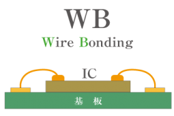
Bare chip bonding on the board
COB is an acronym for Chip On Board. A general term for technologies for bonding chips on a board (PCB board).
Since the semiconductor bare chip is bonded directly on the substrate, space-saving bonding and low-profile bonding are possible compared to bonding packaged products.
There are various methods for connecting to the board, but the most typical method is wire bonding. (Sometimes abbreviated as WB)
What is wire bonding?
A metal wire is used to connect the circuit pattern on the board and the electrode of the chip. The gold wire is joined to the aluminum electrode and gold terminal by heat, ultrasonic waves, and load. The bonding area can be made smaller than that of SMT, and the printed circuit board can be made smaller.
Bonding type
The role of wire bonding is to electrically bond the inside and outside of the IC, and the technologies used include the thermo-compression method, which joins by applying heat and load, and the thermosonic method, which also uses ultrasonic waves. I have.
Bonding process
◎ Ball bonding
A method often used in mass production factories, wires are passed from directly above to directly below a tool called a capillary. You can make a loop in all directions of 360 degrees where it contacts the bonding surface, but you can't use a very thick wire because it make a ball using sparks.
◎ Wedge bonding
A wedge tool is used for bonding. Unlike ball bonding, we don't have to blow sparks to melt the wire, so use can use its wire, such as aluminum wire, in addition to gold wire. Wedges can only be looped in one direction, but we can do bonding with ribbons and thick wires (wires of 100 μmφ or larger).
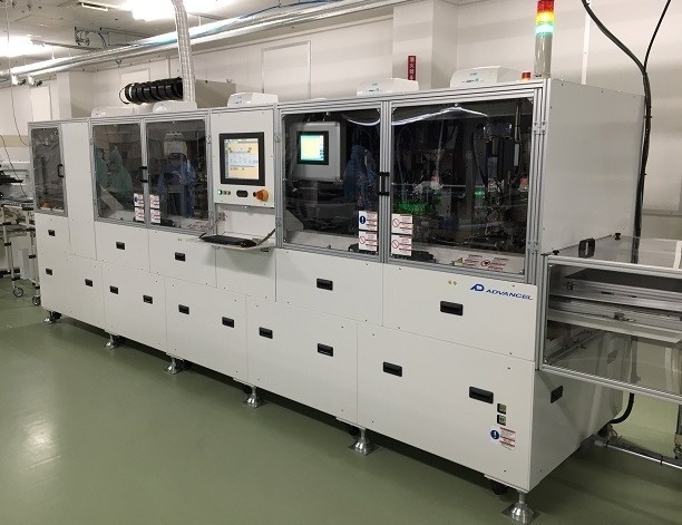
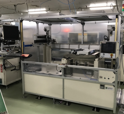
We can handle various types of gold wire, aluminum wire (thin wire, thick wire), aluminum, and gold ribbon. We also undertake a small number of prototypes. We also perform wiring processing for bare chip evaluation and evaluation of board bondability using plasma cleaning equipment.

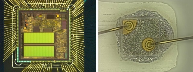
COB wire bonding example of integrated circuit IC (left) and wire bonding example of LED chip (right)
Please feel free to contact us from the inquiry page for various experiments, prototypes, mass production.