Now, bonding the LED on the completed LED bonding board.

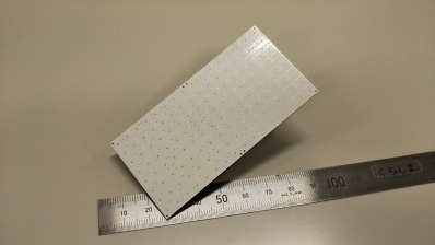
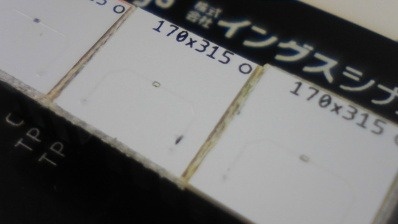
Our miniLED bonding machine requires an alignment mark around the board. This time, as shown in the photo below, they were placed at the four corners of the board and the center of the long side. The area around the alignment mark and the LED bonding part cannot form a resist, so it cannot be a pure white board.
Using this alignment mark, the LED is bonded with a position accuracy of ± 25um (3σ). Therefore, if the alignment mark is not round or scratched, a bonding error may occur.

± 25um is a considerable position accuracy, but since the LED chip itself is 100 to 200um and the connection PAD does not have a 100um gap, some chips may not be able to connect if the accuracy is worse than this. Naturally, the pattern accuracy of the board is also required to be high. In the demo machine, we have devised a pattern design so that even an inexpensive FR-4 board can be used.


Mini LED bonding board (around the alignment mark)

Mini LED bonding board (around the alignment mark)


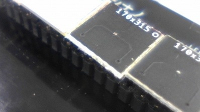
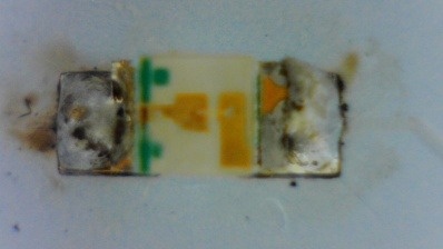
t is an expansion of the LED bonding part.
You can see that the bare chip LED is bonded in the resist opening.

The size of this LED is 0.2 x 0.38 mm. It becomes almost invisible to the naked eye when it is a little away. Compared to the LED size, the size of the copper foil gap and through hole on the board is conspicuous.

A special solder material is used to connect the LED and the board. Print it in the same way as general cream solder and place the chip on it. It is also important to control the coating amount, because if the amount of solder printing is large, it will slip when the chip is placed.


Expansion of mini LED bonding part

Expansion of mini LED bonding part


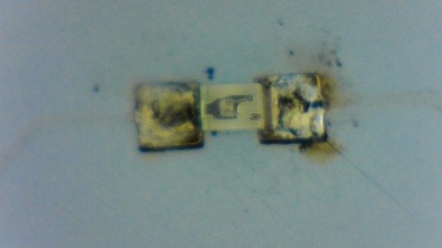
The photo below shows the LEDs bonded at a 5mm pitch from a distance.
This time, the resist was applied once because it was the standard specification of the board manufacturer. If you look closely at the photo, there is a difference between the white part without the copper foil and the white color on the copper foil, and the top of the copper foil is a little pink. If you want more whiteness, you may need to take measures such as printing the resist twice.


Mini LEDs lined up at 5mm pitch

Mini LEDs lined up at 5mm pitch


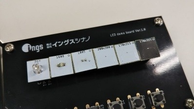
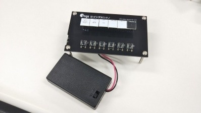
The number of boards we made is 128 chips / board, which is small and easy to install.

Therefore, we were able to use the board we made to practice engineers who handle new mini LED bonding machines.
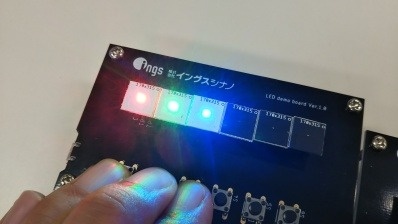
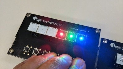
Connect the power supply to the anode terminal and cathode terminal on the back of the board and check that it lights up. Since it is connected in a matrix, somewhere will shine when you hit the probe appropriately.

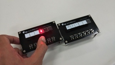
Next is the lighting of the whole.


I am “R” from the Sales Technology Group.

It seems that the main uses of miniLED are backlights and displays.
The backlight has become particularly famous for being adopted in the iPad Pro. We also had a demo machine that imagined a light source for such a backlight, but it was damaged by the activity for many years (?).

Therefore, we decided to make a demo machine with the image of a new backlight source.

The main goals are:

  1. The LEDs are arranged in a matrix and can be freely controlled to some extent.
  2. Being able to handle later when we want to raise a board with a different pitch.
  3. The distance between the LED and the edge of the board should be half pitch on all four sides so that tiling can be performed.
  4. As cheap as possible (important!) and hard to break.

After investigating various things, it was decided that it would be better to use an IC called HT16K33 that can control 8x16 LEDs.
The point we were worried about was that although the Dimming function can be used to control the brightness as a whole, it is not possible to display halftones and the current that flows seems to be a little large. The merit is that it seems to be easy to handle and that many dedicated boards are sold by Akizuki Denshi. Moreover, it costs 250 yen per sheet.
Since the halftone display is not possible because it is a demo machine, we decided to select a current that can pass a certain amount of current. It is a pity that the smallest size (0.1mm x 0.2mm) that we have a track record of handling cannot be used.

And here is the completed board.


8x16 mini LED board

8x16 mini LED board


The LEDs have a pitch of 5 mm, and 128 LEDs in 8 rows and 16 columns can be placed on a single board.
Since the distance to the LEDs on the four sides is 2.5 mm, we should be able to display tiling by arranging these boards side by side. The control program seems to be difficult.

The board is a general FR-4 board. To make it easier to handle as a demo machine, we use a thick board of 1.2 mm.

The point that this board was devised is:

  1. The HT16K33 board sold by Akizuki Denshi was soldered so that it could be used.
  2. Since it is necessary to create a cradle if parts are bonded on the back of the board when bonding the mini LED, the LED driver is bonded after bonding the LED. With this structure, it is possible to handle substrates with different pitches.
  3. It was made easier to assemble by making it possible to connect the power supply / signal line to the adjacent board during tiling.
  4. The wiring can be pulled out as an LED matrix of 16-pin anode x 8-pin cathode so that it can be controlled by other ICs.

and so on.

Next time, we would like to bond the LED on this board and turn it on.


We tried to make a versa writer by applying LED bonding technology. Persistence of Vision (PoV) may be more common overseas.

An image is output by attaching a sensor to the rotating body and controlling the light emission according to the position.


This is “R” from the Sales Technology Group.

This time, we will introduce an example of bonding a mini LED on a transparent FPC.

Due to the size of the mini LED (from 0.1 mm square), the LED alone is almost invisible. Therefore, we thought that if it was bonded on a transparent board, a transparent display could be created when it was not lit.

First of all, please see the operation of the created demo product.


The created transparent FPC uses wiring with a pattern width of 0.04 mm (40 μm).

40 μm wire is thinner than a human hair thickness (50-100 μm).

The ideal is "invisible wiring", but this level of wiring width is usually the limit when creating an FPC.
In the capacitive touch panel, there is an example where wiring of about 4 μm, which is an order of magnitude thinner than this FPC, is used. In addition, blackening may be applied to make the copper color less noticeable, and if the panel is made with such technology, the wiring will be almost invisible. However, if the wiring is too thin, it will not be possible to pass current, so it may be necessary to balance visibility and current capacity.
In the panel created this time as well, the matrix-driven common electrode concentrates the current of 18 LEDs, so three 40 μm wide wires are connected in parallel.


The LED bonded on the FPC can be easily removed by external force if it is left exposed.
Since the chip size is too small, the connection area is small and the strength is inevitably low.
Therefore, to protect the chip, we covered the LED with a slightly thicker OCA and transparent film. The LED chip itself is about 0.1 mm thick, and we used a soft OCA with a thickness of 1.0 mm to ensure that the area around the chip is filled with OCA and that no external force is applied.


Since both FPC and protective film are bendable materials, we were able to create a transparent display that can be bent as shown in the photograph.

Normally, even if a hard LED chip is bonded on the FPC, bending the bonding part will destroy the bonding part, so it is better to avoid it. In the case of a mini LED, the chip size is small, so even if the FPC is bent, the displacement of the chip is not large, and the protective film and thick OCA do not seem to peel off easily.

We would like to make a transparent electric bulletin board by arranging a lot of LEDs on a larger board, but there is a budget for making a demo product, so it is on this scale.
Since the mini LED itself can be bonded on a 30 cm square board, it can also be bonded on a large board. You can also make a larger display by tiling. If you are interested, please let us know.


This is “R” of sales technology.

We would like to introduce a demo set of 0.1mm class size LEDs, which are mini LEDs that you rarely have the chance to see, so that you can turn them on one by one and check their appearance.

Here is what we made.


Can you see the small white and black square boards lined up on top of the black board lined with switches?
Various LEDs are bonded in the center of this small board.
The current limit uses a constant current diode (CRD) and is a constant current of 15mA (cut out).


The small board is replaceable so that various comparisons can be made.
This is the one that allows you to check the difference in package (size).

From the left, a 3mm bullet-shaped package, 1608 size SMD chip LED, 1005 size SMD chip LED, 0.2mm x 0.3mm mini LED, 0.17mm x 0.315mm mini LED. The ones placed on the white board are lined up, and on the far right, the one with the 0.17 x 0.315 mm mini LED bonded on the black board is inserted.


Here, only mini LEDs of the same size (0.17 x 0.315 mm) are lined up.
R, G, B can be compared side by side.

Here is how it was turned on.


The LED on the white board looks brighter because the board itself becomes a reflector.

On the other hand, the LEDs on the black board are inconspicuous when not lit.

Each has its own characteristics, and even with the same LED, the appearance will change, so you can check them side by side.
The pictures below are enlarged pictures of each.


Actually, we wanted to line up the smallest LED that we could get, 100um x 200um, but the PCB maker couldn't resolve it enough and couldn't install it.
Since the plan was L / S = 3 / 3mil, we were wondering if the recommended land-to-land gap of 80um would be just fine.

Even with the matrix display lighting board that we created earlier, we received a give-up declaration from a PCB manufacturer different from this time, so the point is to make a board for 100um class mini LEDs (if it is an FPC or glass board, it is completely we can make a board without any problem).

Finally, we would like to introduce the difference from the SMD package product.
The finish is not beautiful because I mounted it by hand soldering. .. ..


1608 チップLED


1005 チップLED


The top two are 1608 and 1005 SMD types. The land shape is the land recommended by the manufacturer.
Since the land size is a little large, it may be a little disadvantageous for visual comparison.

And the photo below is a 170x315um mini LED. (The magnification has not changed!)
Since the bonding terminals are on the underside of the chip, resist openings are also minimized. Therefore, the presence of the light emitting source can be considerably reduced. A feature of the mini LED is that it is as thin as 100um.


It's a small detail, but this time we made it possible to drive with batteries.
It can be powered by batteries or a USB port. This ensures that when we introduce the demo set to our customers, we won't have to worry about short cables or poor routing.

If you are interested, please contact us using the inquiry form on our website.
We also rent out this demo set.

We are looking forward to hearing from you.