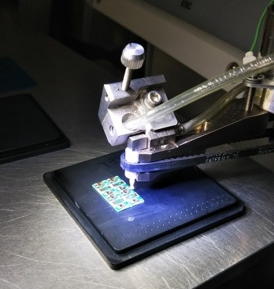
It is “R” of sales technology.

As a countermeasure against the new coronavirus, we can see acrylic plates and transparent film curtains here and there.

Physical partitions are the best way to prevent splashes, but in the hospitality industry, it is desirable to eliminate visual obstacles as much as possible in order to get closer to the customer.

So, as an introduction to our laminating technology, I made a sample of a low-reflection film (AR film) bonded to an acrylic plate.

First of all, from the state without AR film.


The view of the front (your side) is reflected on the acrylic board, and the visibility is not good.

We laminate an AR film on it.
Reflection on the acrylic plate occurs on the front and back of the acrylic plate (air / acrylic interface, acrylic / air interface). For this reason, AR film is laminated on the front and back of the acrylic plate.

Then, it was confirmed that the reflection was almost eliminated.


If you look closely, the reflections are not zero, they look faint, and you can see some coloring.

In addition to the reception booth, why not laminate a low-reflection film on the display case to prevent reflection?

However, "low-reflection acrylic plates" with anti-reflection coating directly applied to the acrylic plates are commercially available. In terms of cost and finish, we recommend that you consider partitions and cases that directly use low-reflection acrylic plates.


At our company, we process the film to be laminated to various parts, not limited to displays.
In addition to the AR film introduced this time, we have a track record of handling films with various functionality.
In addition to flat surfaces, we also laminate to curved parts such as curved plates.

We accept orders from one prototype, so please feel free to contact us.


This is R from the Sales Technology Group. This time, it's just the text, not the series we made.

It seems that the 5G service has started and the service area is gradually expanding.
Speaking of 5G, it seems that it is characterized by high speed, low delay, and multiple terminals, but it is also a big feature that it is used up to high frequencies.
At present, in Japan, the range of 3.6GHz to 4.6GHz of Sub6 and 27GHz to 29.5GHz of millimeter wave seems to be the frequency band of radio waves used for 5G.
By the way, 4G (LTE) uses each band from 700MHz to 3.6GHz, and will use higher frequencies.

With 5G, the frequency used is high, so the size of the antenna is also small. One wavelength of 4GHz is 7.5cm, and one wavelength of millimeter wave is 1cm. Most antennas are about 1/10 to 1λ in size, so it is likely that you will need to use an antenna that is several millimeters to several centimeters in size.

Radio waves with high frequencies will have characteristics closer to light, and will not wrap around obstacles such as buildings and will not reach the radio waves. Therefore, it is said that antenna technology is important in 5G.

On the other hand, "metamaterial" that we wrote in the title.
"Meta" means "transcendent" and refers to materials that have properties that do not exist in nature. The relative permittivity and relative magnetic permeability have a vacuum of 1, and there is no substance smaller than that, but with proper material design, these values are smaller than 1 for radio waves of a specific frequency. It seems that it is possible to create something that can be negative (an area that we can not keep up with as a shallow student).
What happens if that happens is that it will be possible to completely reflect radio waves and diffract them without loss, and we are vaguely wondering if this metamaterial can deliver 5G radio waves to a wide range. However, we are sure it is being researched and developed all over the place.

For metamaterials, it is necessary to make a metal structure that is about a fraction of the length of the target wavelength. It seems that various studies are being conducted on sticks and rings.
This "size smaller than the wavelength", light has a nanometer-sized structure, which seems to be difficult, but at a frequency of about 5G, it is about a few millimeters to a few 10 millimeters. Isn't it within the range that can be made by printing?
We think that various characteristics can be obtained by stacking metamaterial structures arranged on a flat surface by printing.

It's finally (really finally) our turn.
Antennas and reflectors should not have a presence, so we think that patterns may be created on transparent film or glass.
We are good at laminating such members with high positional accuracy, multi-layered, and laminating between various materials. We think that the base material and bonding material may be special in order to suppress the loss of high frequencies. You can also use our equipment to evaluate newly developed materials.
Weird bonding and materials are welcome (at least for business), so please let us know.


Continuing from the previous session.

We bonded the LED.

First, we decided to use anisotropic solder as the bonding material. Anisotropic solder is a material in which solder particles are dispersed in a thermosetting resin. By heat treatment, the solder particles aggregate and melt to form an electrical connection, and at the same time the resin is cured. It is a material that is also mechanically fixed.

First, apply a paste-like anisotropic solder material.


here are two small lands on the right side of the silk-printed letter "S", and the paste is applied to them. Using a dispenser, apply the same amount of solder paste to the anode and cathode as much as possible.

Place the LED on this. Since the LED is small, we use a mounter.


This is a manual operation mounter.
Finely adjust x, y, and θ while checking with a microscope, and mount the chip.

The photo below shows what it looks like after it is placed.
Since the LED electrodes are formed under the chip, you cannot see how they are connected.


The board this time is a general-purpose board. Therefore, the mounting position is also a measure.

We checked the LED specifications in advance and measured the gap between the electrodes on the board, so it seemed unlikely that there would be a short circuit, but there is a possibility that a short circuit will occur with cream solder or silver paste. Was not zero, so we used anisotropic solder.
Even if anisotropic solder is applied across narrow electrodes, the risk of short circuit is less than that of isotropic conductive materials (conductive paste, solder, etc.) because the solder particles aggregate during curing.

All that remains is heat treatment.
Hold in the oven for the specified time and temperature conditions to complete.


Lights up safely!

We thought that the 1.1mm square might have a bonding defect, but we were able to confirm that all of them were lit.


How was that.
This time, we introduced the bonding scenery for individual evaluation using a large LED among the mini LEDs. As LEDs become smaller and become about 0.2 mm square, the selection of connection materials becomes more careful, but as a result, 0.2 x 0.1 mm LEDs can also be bonded with a high yield.

In this way, we also undertake a small amount of bonding for evaluation, so please do not hesitate to contact us from the Web inquiry form.

(End)


It is R of sales technology.

This time, we would like to introduce "We also accept such evaluation bonding".

This time, we asked a customer who said, "I want to evaluate a mini LED, and I got a chip, so I want to do a basic evaluation."

We received a consultation as to whether the LED chip could be bonded on a commercially available board as shown in the photo.


LED and evaluation board

LED and evaluation board


For ordinary SMT devices, lead wires can be soldered to the terminals for basic evaluation. However, it is quite difficult with bare chip LEDs.
The white square in the photo is the LED chip. The one in the picture is 1.7 mm square size, and they wanted to evaluate two types of LED chips, this size and 1.1 mm square.

The evaluation board is a general-purpose (commercially available) chip LED evaluation board, and it seems that 1.7 mm square can be mounted, but the 1.1 mm square chip does not seem to match the PAD on the chip and the PAD on the board.

For the time being, we will try to connect with the materials we have.
In the case of a 0.1mm size mini LED, the connection material is also a fairly severe selection, but since it is a 1mm class, there seem to be many options. First of all, we decided to try the silver paste and anisotropic solder paste that we have in stock.
Due to the small quantity, the work is manual.

(Continue)


(Continued from last time)

Arrange the four completed FPCs in a horizontal row.
Since there is only 0.1 mm between the LEDs, the connection between the FPCs must be 0.1 mm or less, and the FPCs must be disconnected and connected.

We carefully cut and connected while looking into the microscope.

Laminate it on a transparent acrylic board and the demo set is complete!


For the convenience of the control board, a black hidden plate is placed under the light emitting part.

This caused a lot of misunderstandings at the exhibition and was a bit of a failure.
We received many inquiries such as "Does this black part shine?"

It would be great if the black part actually became a full-dot display. .. ..

This time, four driver ICs control 800 LEDs.
In order to make this a display, it is necessary to prepare hundreds of sets of the same thing or another driving method, which is quite a hurdle for us as a bonding contract service.

Please also see the video that shows how it works.


The board produced this time supports up to 1600 LED control.

We were worried whether the processing power of the microcomputer would be okay.
At first, when we confirmed that all the LEDs were lit, it took seconds to rewrite the lighting contents of all the LEDs, but we read the driver IC specifications carefully and optimized the writing method several times. Or, using DMA, it's 100x speed, and now it's probably about 100fps.
Software is important, isn't it? we learned a lot.

This is the end of the introduction of the miniLED bonding demo product.
We are bonding LEDs and other devices.

We are also developing a demo machine for this scale exhibition, so please feel free to contact us.

(End)