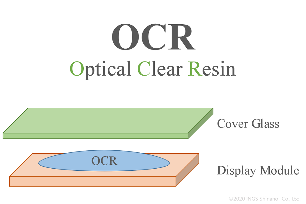
OCR is an abbreviation for Optical Clear Resin.

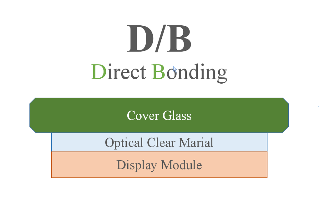
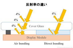
If there is an air layer between the display and the cover glass / touch panel, etc., the appearance will deteriorate due to interfacial reflection. To improve its appearance (to reduce interfacial reflection), the space is filled with a material with a refractive index close to that of the material to be bonded. OCR is one of the materials that fills the space.

For details, see "About direct bonding".


Features of OCR


OCR is initially liquid. At the time of laminating, OCR is applied to the panel and then laminated to the opposite panel.

The merit for OCA is that if there is any misalignment or foreign matter at the time of laminating, it is easy to rework if it can be found before curing. Also, compared to OCA, the material cost seems to be cheaper because there is no sheet processing or outer cut.
In addition, since it is filled with liquid, it can absorb different shapes as well as printing steps on the cover glass.
However, since it is a liquid material, care must be taken when handling it. In particular, it is known that if it gets into the gap of a material that you do not want to enter when it is uncured, it will cause problems such as display problems later.

About the process

In the OCR method, a liquid is applied to one panel and the opposite panel is brought closer to bond.
Many OCRs are designed to cure with UV (ultraviolet) light, so a spot light source cures the resin (temporary cure). After that, UV is applied to the entire surface to promote the reaction as a whole and bond.
In addition, there are many variations such as two-component curing type, thermosetting type, and combined type of each.

Ings Shinano has a long track record of handling a wide variety of OCRs.
Please feel free to contact us.


What is direct bonding?

When stacking a cover glass or touch panel on a display, if an air layer is sandwiched between them, the interfacial reflection between the air layer and the panel will reduce the brightness of the display and increase the reflectance, resulting in deterioration of the appearance. In particular, when it is not lit or when it is displayed in black, reflection by external light increases, so black floats and the contrast deteriorates, and the difference from bezel printing becomes noticeable, resulting in deterioration of quality.


In order to improve this appearance, direct bonding is the process of removing the air layer between the display and the cover glass or touch panel. Instead of the air layer, it is filled with a transparent resin with a refractive index close to that of the display or cover material (glass, acrylic, etc.) so that there is almost no interface optically. For this reason, direct bonding is also called optical bonding (optical bonding) or optical direct bonding.


Types of direct bonding


Direct bonding can be roughly divided into two methods depending on the material of the adhesive layer. These are OCA (optical transparent double-sided tape) and OCR (optical transparent resin). Each has advantages and disadvantages, so we will use them properly according to the product.

We can process not only display devices but also direct bonding of various parts.
We support small-scale trial production, such as when you want to try only one piece in the appearance evaluation, so please contact us by phone or inquiry form.

Effect of direct bonding

As explained at the beginning, the purpose of direct bonding is to improve visibility by performing optical bonding.

How effective will it be?


The figure is a schematic diagram of a comparison of reflectance between direct         bonding and sandwiching an air layer.

Glass and air have different refractive indexes, resulting in about 4% interfacial reflection.

In direct bonding, the incident external light is reflected by the outermost surface and the display surface of the display.
Most of the display surface is black (normally black) due to polarizing plates and black masks, and the reflectance is about 4%.

On the other hand, in the case of an air gap, there are two air / glass interfaces and one air / display interface. Since each has about 4% reflection, the total reflectance is about 12%.

This difference is the difference in visibility between direct bonding and the air gap.

Furthermore, it is possible to reduce the reflection on the outermost surface by applying AR treatment to the surface of the cover material or attaching an AR film.
In the case of an air gap as well, in order to reduce the reflection of the air layer interface on the inner surface, we may aim to improve visibility by using AR or moth-eye structure.

We can also handle the laminating of AR film and moth-eye film, so please feel free to contact us by phone or using the inquiry form.


Bare chip bonding on the board

COB is an acronym for Chip On Board. A general term for technologies for bonding chips on a board (PCB board).
Since the semiconductor bare chip is bonded directly on the substrate, space-saving bonding and low-profile bonding are possible compared to bonding packaged products.

There are various methods for connecting to the board, and one of them is ACF bonding. Place the ACF on the board and mount the chip on it with flip chips. The chip is bonded on the board by thermal crimping of ACF.

It is suitable for adhesion between ICs and boards that require continuity between opposing circuits and insulation between adjacent circuits.

ACF (= Anisotropic Conductive Film) is an abbreviation for Anisotropic Conductive Film, which is a sealing resin in which conductive particles are dispersed in a thermosetting epoxy resin. By heat crimping, it exhibits electrical anisotropy that maintains conductivity in the thickness direction and insulation in the plane direction at the crimped part.


ACF contributes to the miniaturization and thinning of electronic components.


When bonding an electronic component, ACF is sandwiched between the electrode part of the printed circuit board and the electrode part of the component, and the component is pressurized while applying heat. Then, the conductive particles dispersed in the film are crushed between the electrodes and eventually form a conductive path. Uncrushed particles remain dispersed in the resin, preserving insulation. As a result, an anisotropic conductive path is formed between the electrodes in the vertical direction and insulating from the adjacent electrodes in the horizontal direction. In addition, the resin in the ACF is cured to hold the conductive particles and mechanically fix the bonded parts.

This makes it possible to mount electronic components without causing a short circuit even if the distance between the electrodes in the lateral direction is narrow.


We accept ACF (anisotropic conductive film) bonding prototypes!
Please feel free to contact us from the inquiry page.


What is a flip chip?

Flip-chip bonding is a method of bonding a bare chip (a semiconductor cut out into a chip) by inverting (flip) it.
Before the advent of flip-chip bonding, wire bonding was the mainstream for semiconductor bonding. Since wire bonding connects the chip and the substrate with a wire, the active surface of the chip was the upper surface. On the other hand, in flip-chip bonding, the active surface faces downward and is mounted facing the board surface. It is called a flip chip because the chip faces the opposite side of the wire bonding.

Flip chip bonding features

Comparing flip-chip bonding and wire bonding has the following advantages.

  1. Space saving compared to wire bonding
  2. Wiring length is shorter than wire bonding, and there is less inductance component (suitable for high frequencies)
  3. Since it is directly connected, the resistance value is low and the loss is low.
  4. Since the terminals are connected at once, the throughput is high in the case of multiple terminals.

Application of flip chip mounting

Flipchip bonding can be applied to various locations such as bonding on an IC package, bonding on a PCB board, and connecting a multi-chip IC to an interposer.

Flip chip bonding process

In flip chip bonding, a semiconductor chip is bonded with high accuracy using a dedicated bonding machine (flip chip bonder).
In addition to ACF connection, electrical connection is made by ultrasonic connection.
Ings Shinano supports flip-chip bonding with ACF connection.

We accept small-scale prototype service for flip chip bonding!

We accept advanced flip chip bonding, prototyping, joint reliability evaluation, etc.
We can handle from one flip chip to trial production to mass production in a short delivery time. Please feel free to contact us for more information.


We are capable of high precision die bonding and ACF boning! We can handle from one flip chip to trial production to mass production in a short delivery time. Please contact us for more information.


IH spot reflow is a technology that uses induction heating (IH) to locally heat only the metal part and perform soldering.
Since it is heated by induction heating, only metals such as solder and leads generate heat.

There are two advantages of this IH spot reflow system.
First, the heat effect on the base material to be soldered can be minimized. Electronic components can be bonded on materials with low heat resistance such as PET film, cloth, and paper.
The second merit is that it can be applied to repair applications, such as melting and removing the solder only for parts in narrow areas, taking advantage of the fact that it can be heated locally.


We are collaborating with Wonder Future Corporation to evaluate the introduction of the IH spot reflow system.
https://www.ings-s.co.jp/information/products/entry-307.html

Please contact us if you are interested, or if you are considering solder bonding on a low heat resistant base material, solder bonding by local heating, repair, etc.