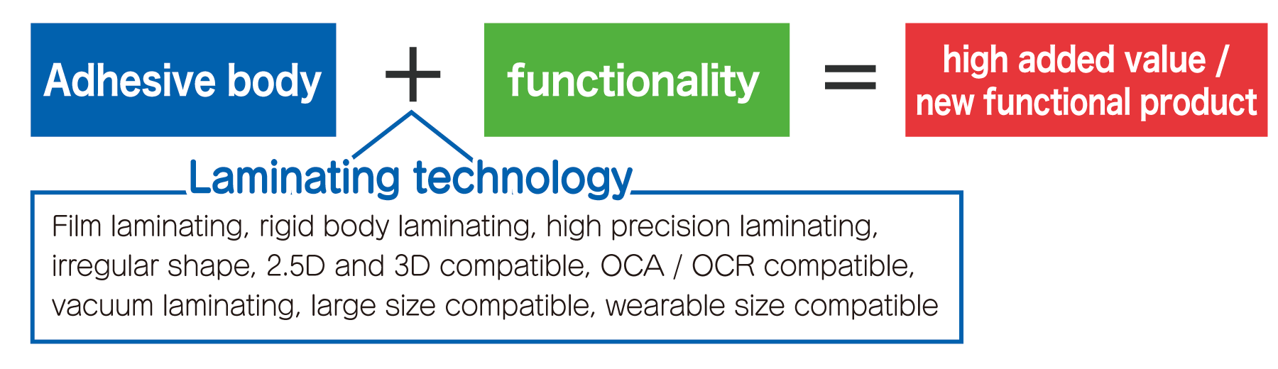
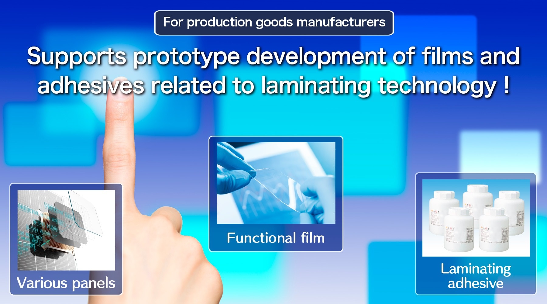
Laminating technology that creates high added value and new functions
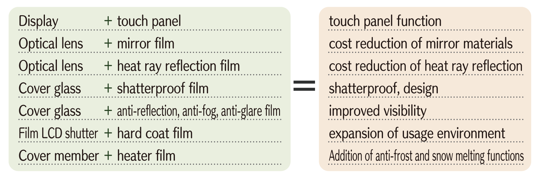
Example of laminating
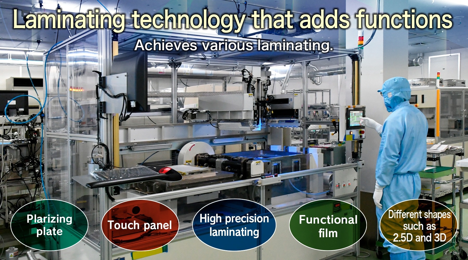
We can help you add value to parts and products using our laminating technology.
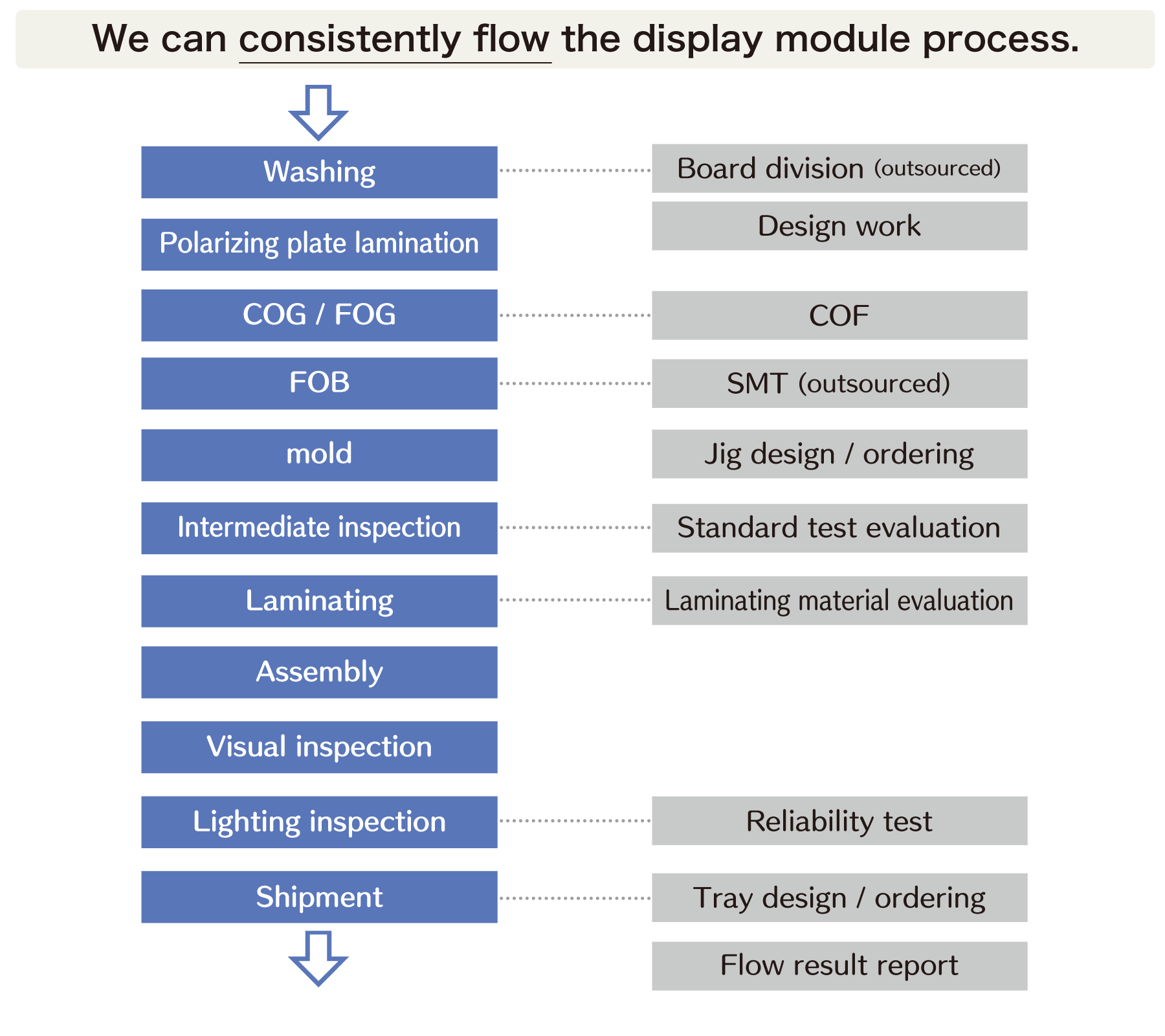
With our automatic laminating machine and vacuum automatic laminating machine, it is possible to handle a wide variety of flat panel displays.
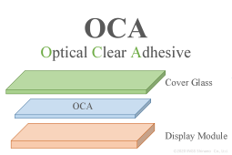
We have a track record of supporting high-precision polarizing plate laminate to panels, film laminate to glass, direct laminating (OCA method / OCR method), and film-to-film laminating.
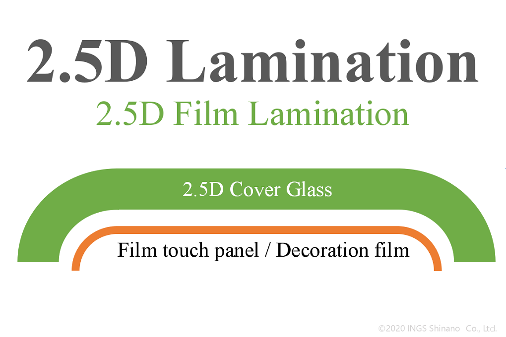
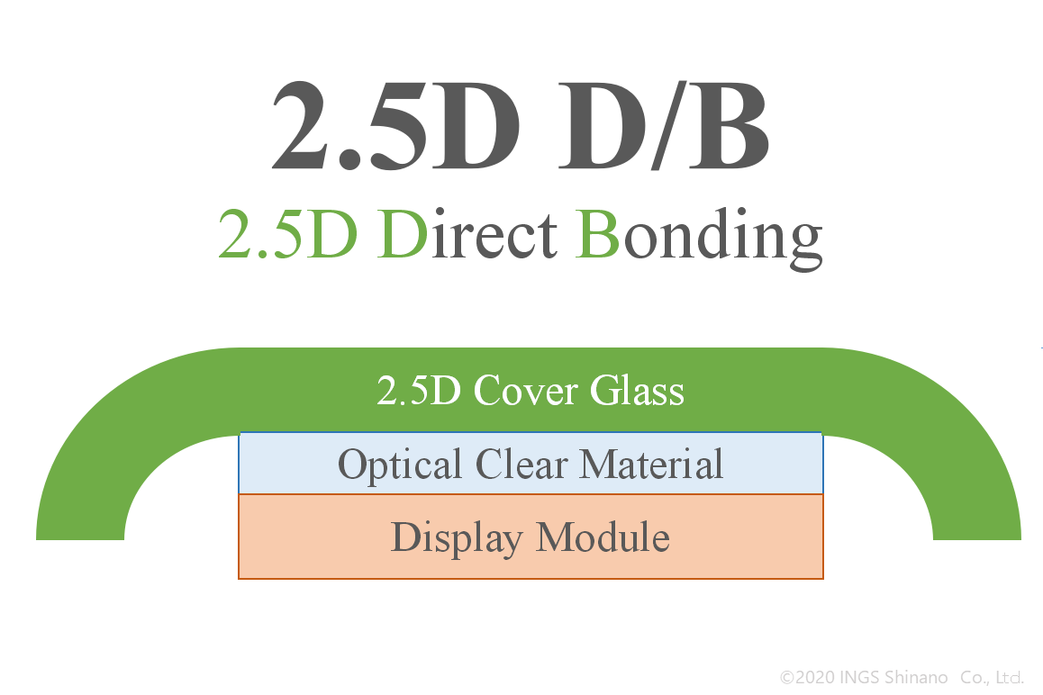
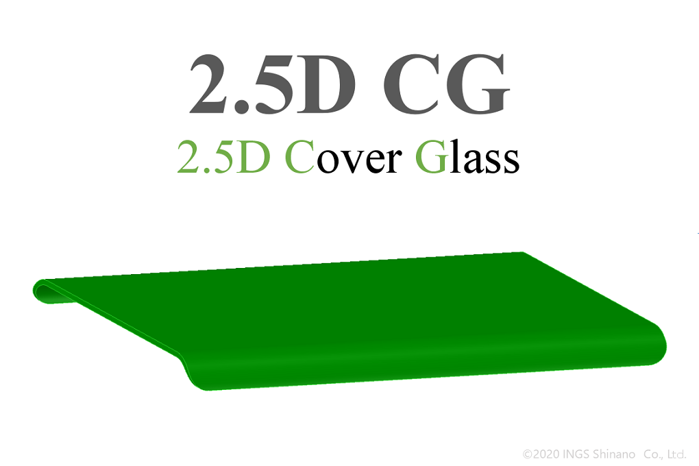
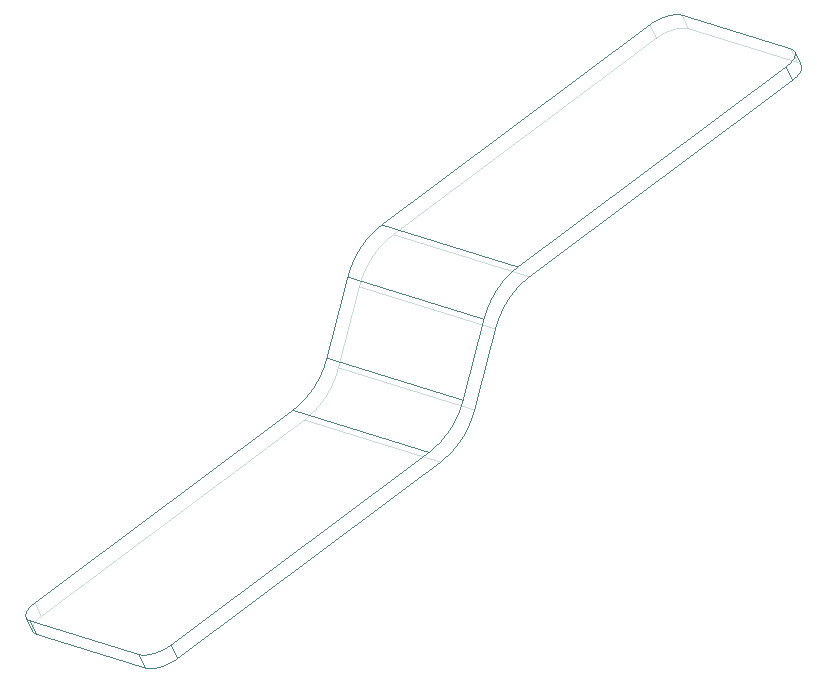
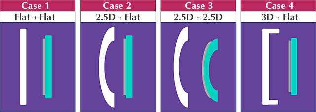
We support not only laminating of flat plates, but also laminating to 2.5D and 3D shapes. Please feel free to contact us as the restrictions will change greatly depending on the shape.
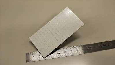
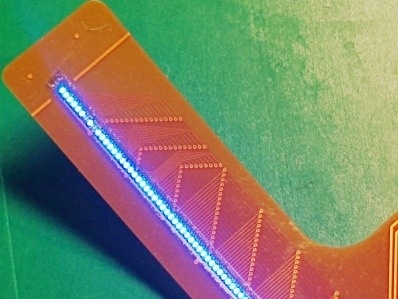
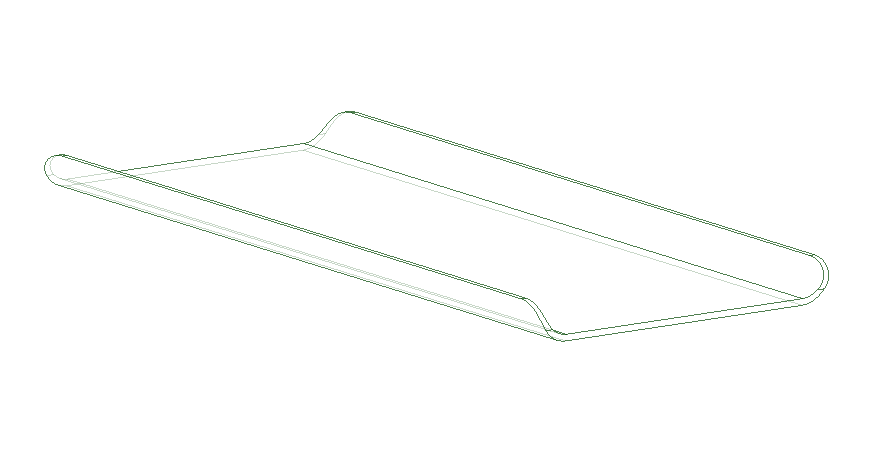
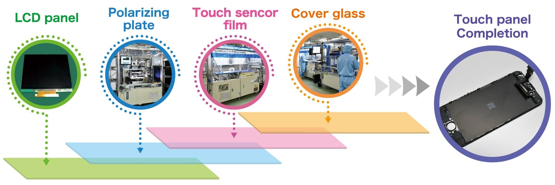
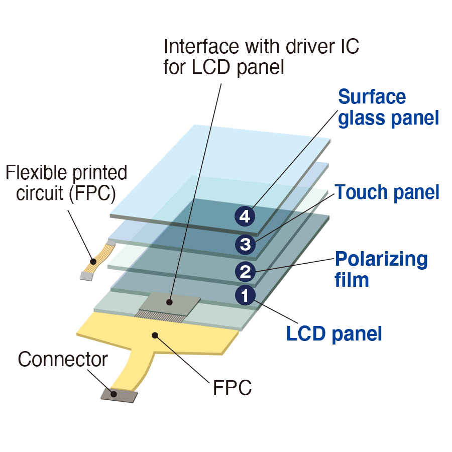
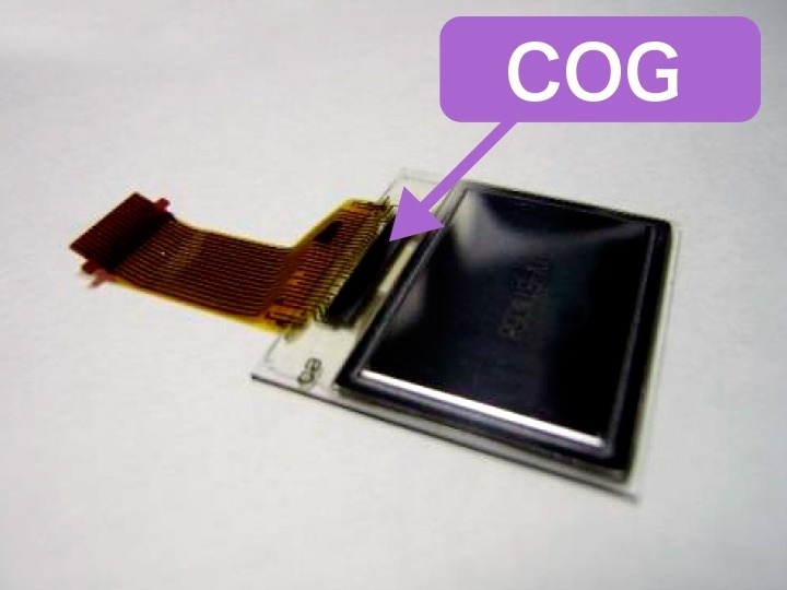
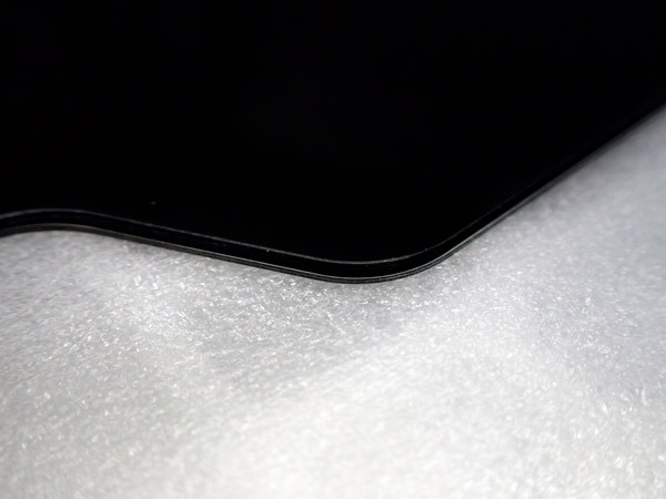
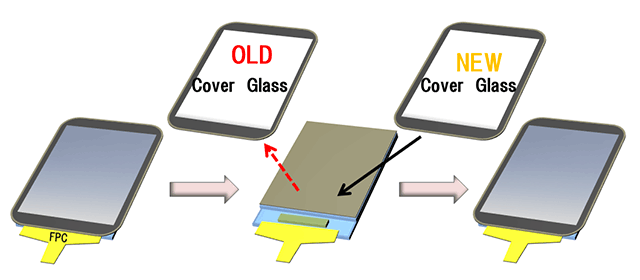
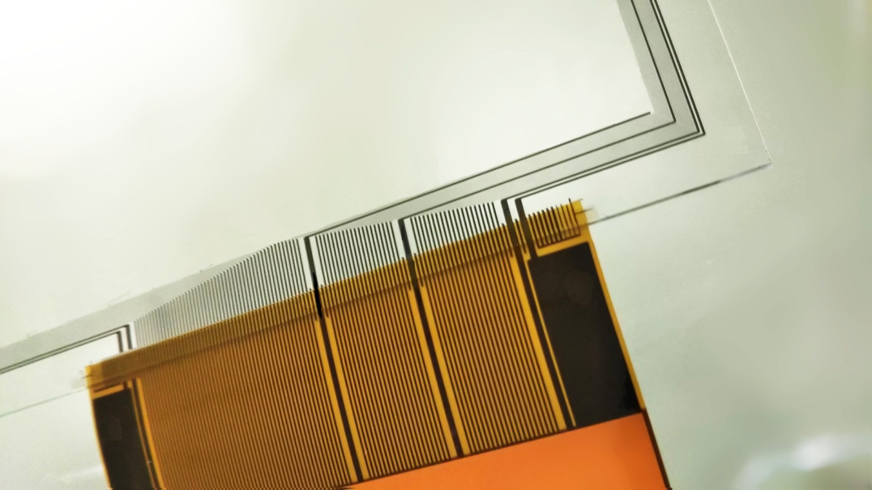
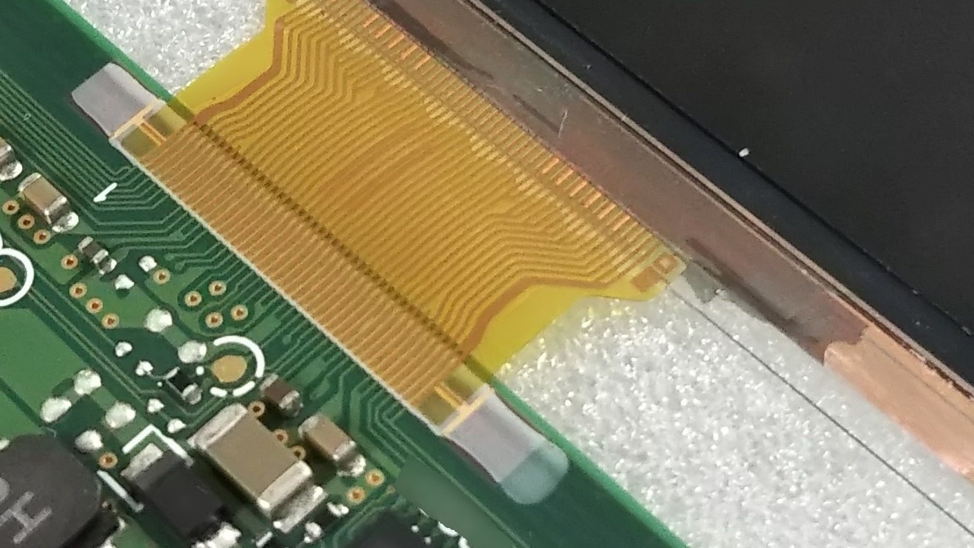
Laminated image (LCD panel with touch panel)
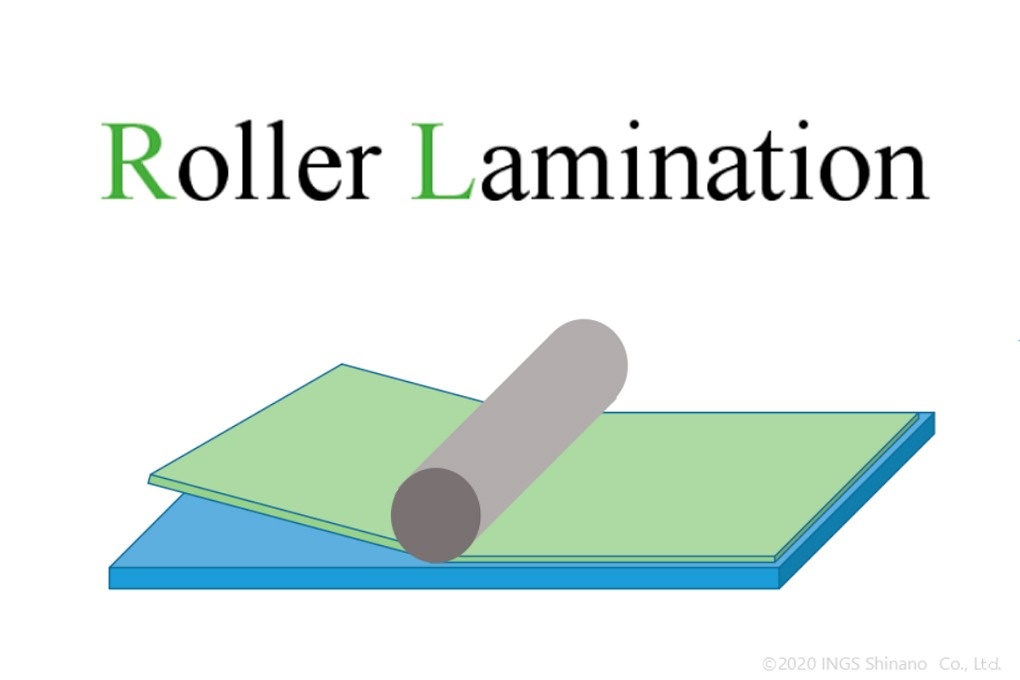
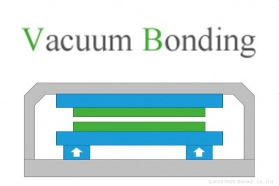
Various laminating technologies
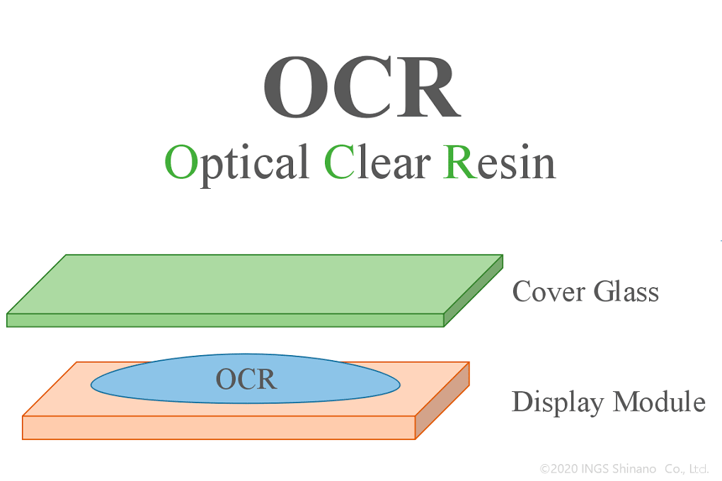
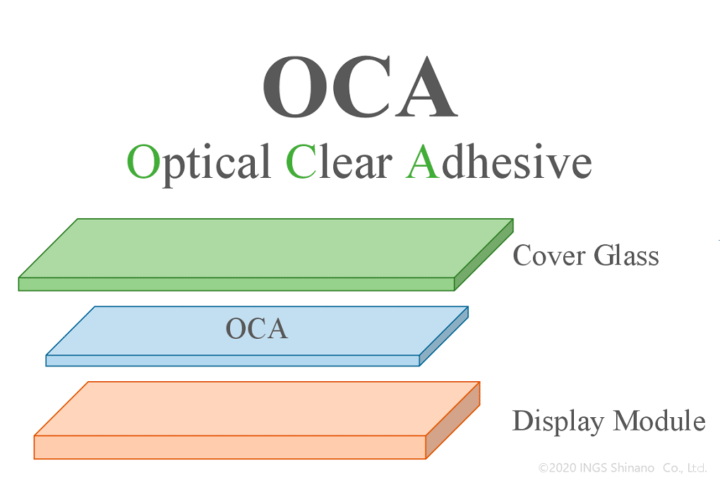
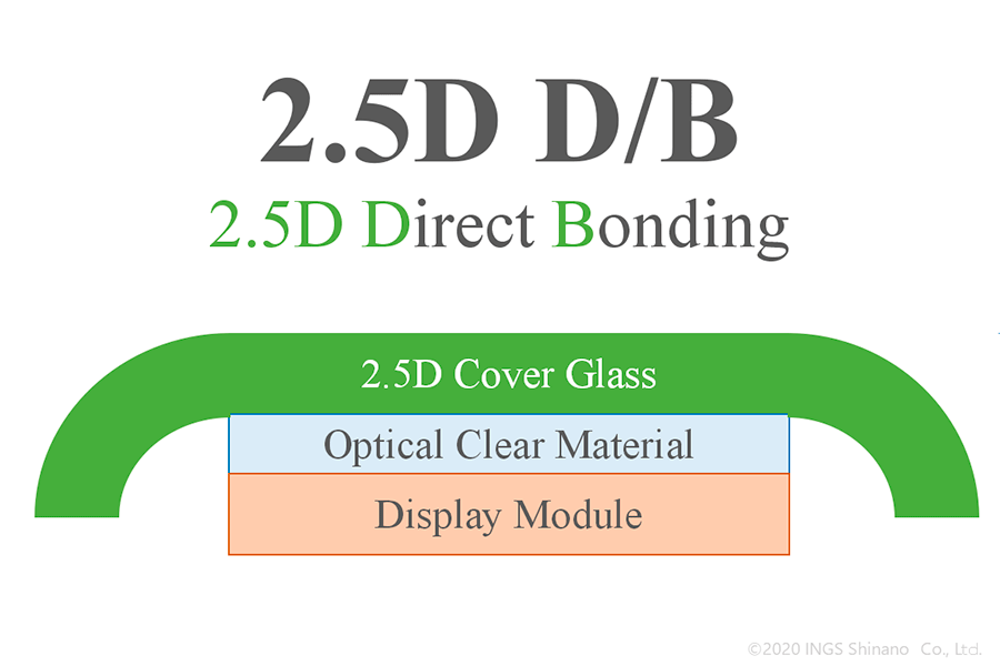
Direct laminating
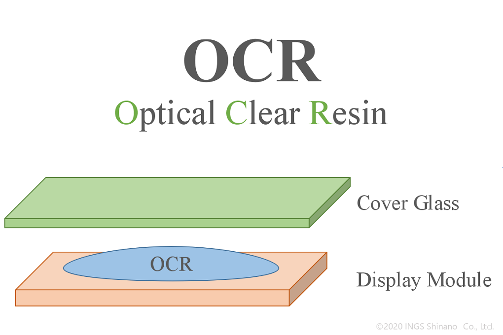
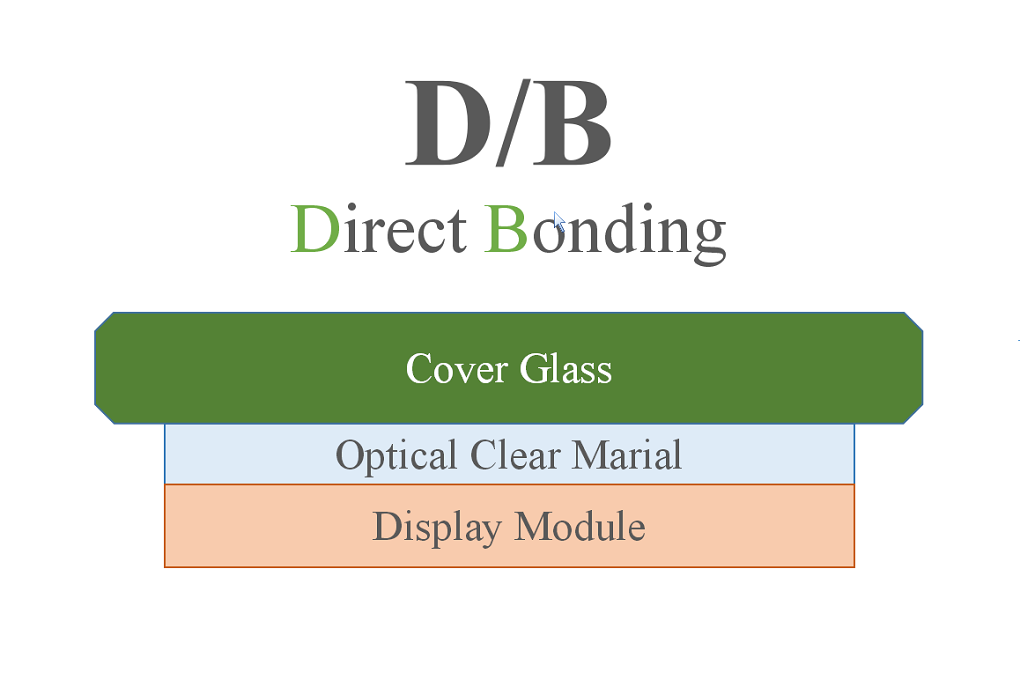
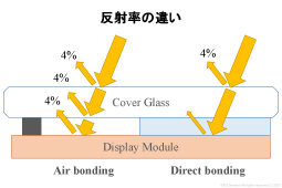
Laminating of optical materials between rigid bodies such as displays and cover glass is called direct laminating (optimal laminating).
It supports a variety of sizes, from small 1-inch displays to TV sizes.
Direct laminating compatible size
・ OCA (up to 47 inches)
・ OCR (up to 12 inches)
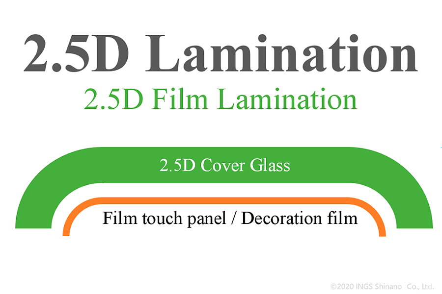
Film laminating
In addition to laminating polarizing plates, various functional films are also laminated.
With a large number of owned machines, it can be used for a wide range of applications such as laminating large films and high-precision alignment.
Flat / curved surface laminating technology
In addition to flat plates, we also accept lamination on curved surfaces.

laminating type
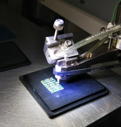
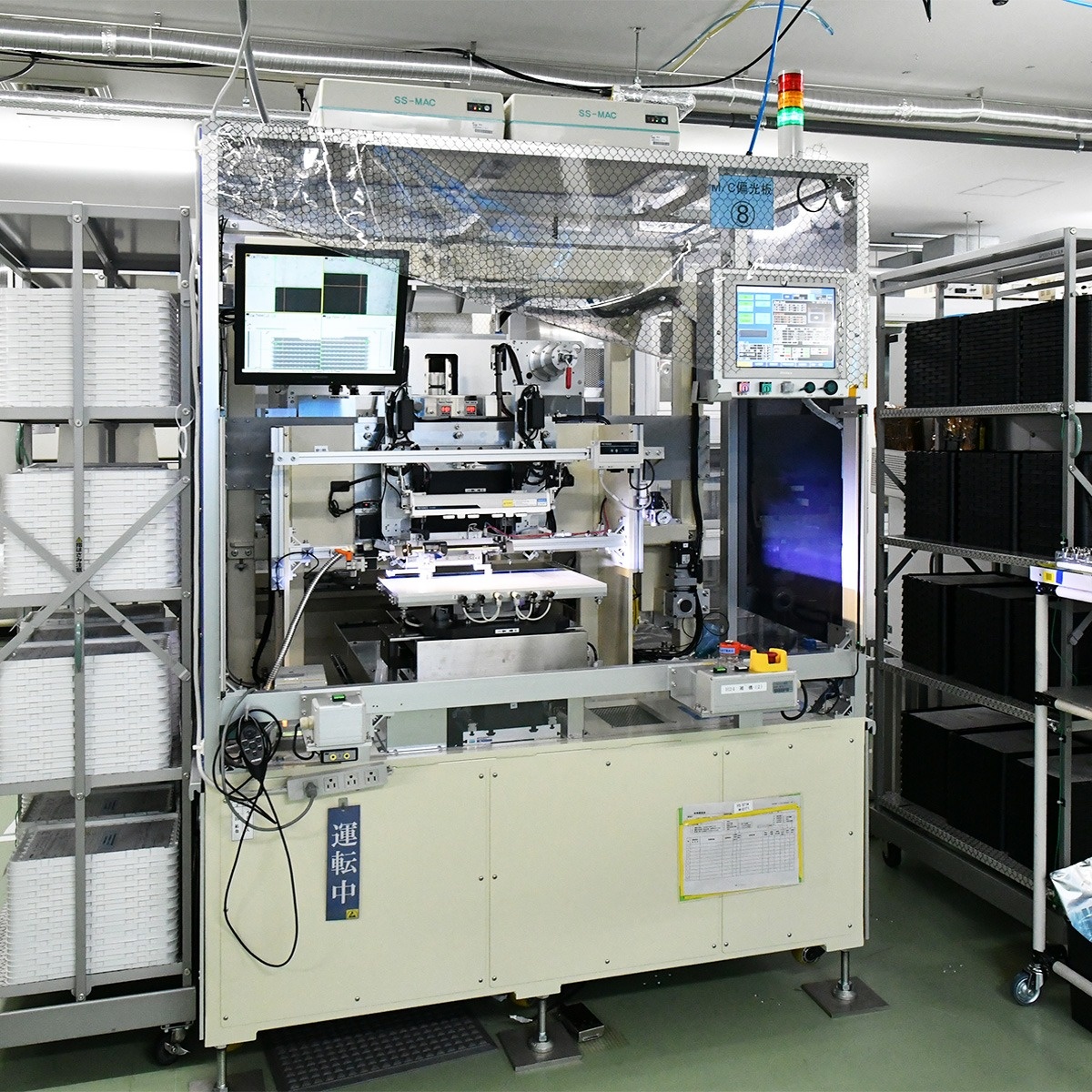
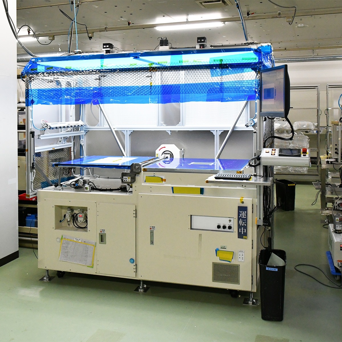
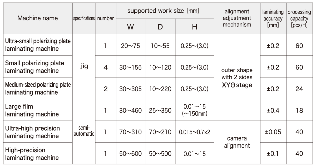
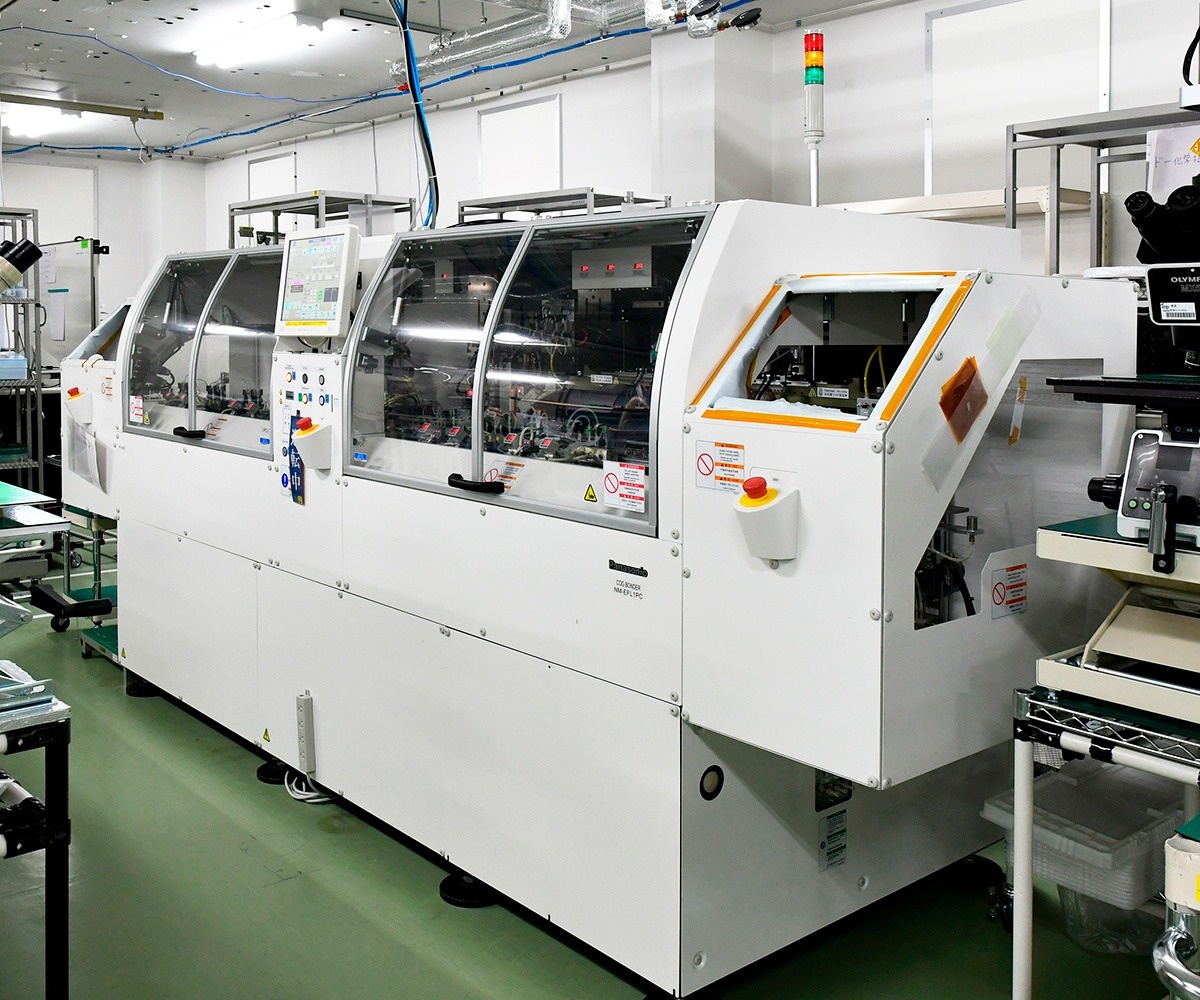
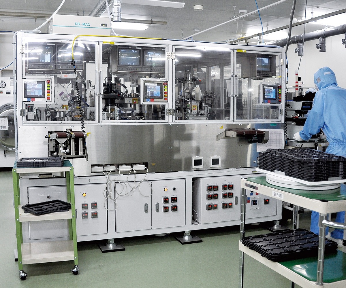
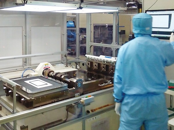
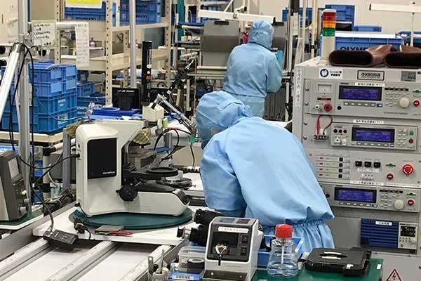
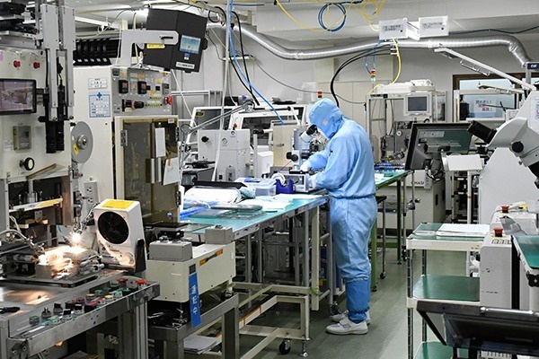
Laminating machines
The highly versatile laminating machines make it possible to flexibly respond to customer prototype specifications.
In order to realize highly difficult laminating, we will realize laminating from abundant experience such as equipment modification and process construction.
High-precision laminating machine
Basic specifications
- Corresponding panel size: 4 to 13.3 inches
- laminating accuracy: ± 0.05 mm
- Work holding with a holding sheet that does not allow air bubbles to enter the front and rear ends
Semi-automatic sheet-fed laminating machine (high precision type)
Basic specifications
- Telephoto type with auto-alignment function
- Laminating accuracy: ± 0.05
- Corresponding size: W500 × L600 × T (total height) 15mm
- Weight: up to 3 kg
- Please use it for bonding various thin materials such as touch panels, cover glass, protective films, etc.
- If the curvature is loose, 2.5D (kamaboko type) support is also possible.
- Conditions vary depending on the object, so please contact us each time.
Remarks: Ultra-high precision laminating machine = alignment mark can be recognized / High precision laminating machine = edge detection
Features: Compatible with 1-29 inches, maximum accuracy ± 25μ, sensor film, OCA, decorative film possible
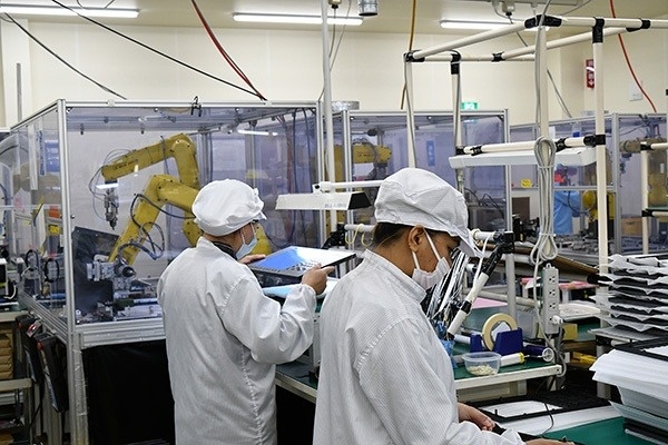
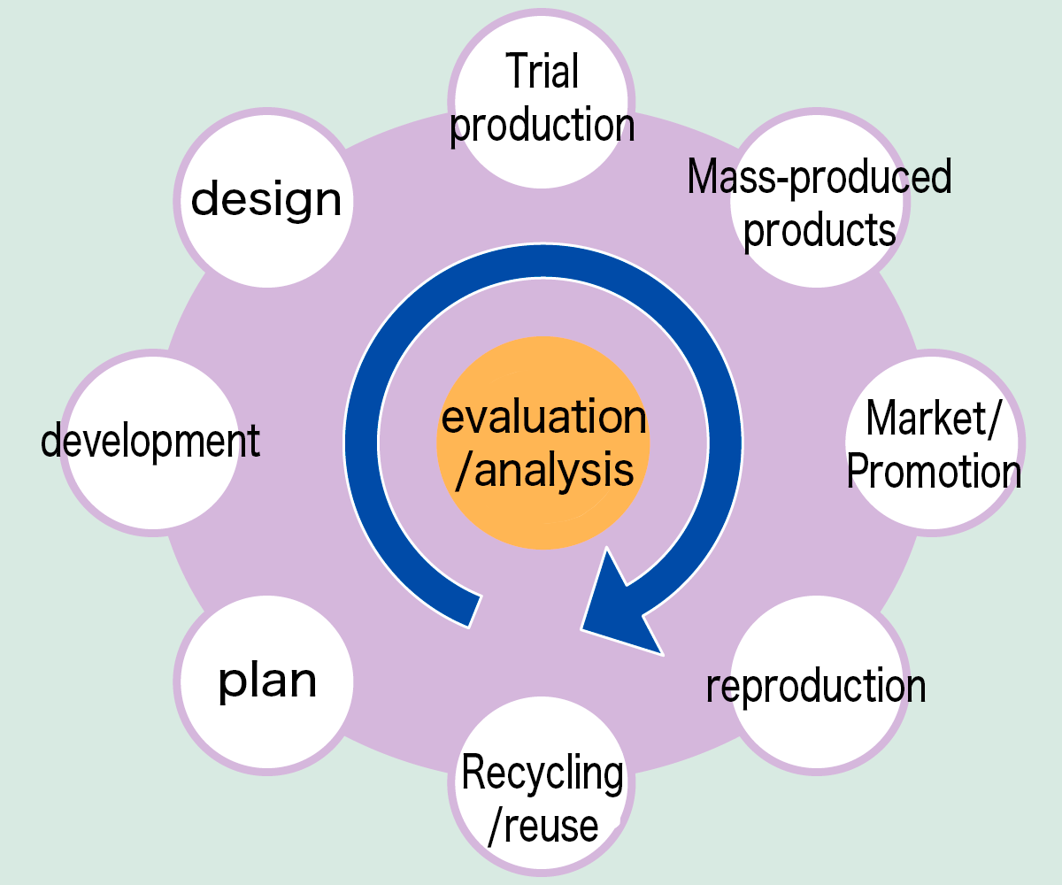
Technical issues related to laminating and trial production consultation
We will help you solve the problems of laminating technology.
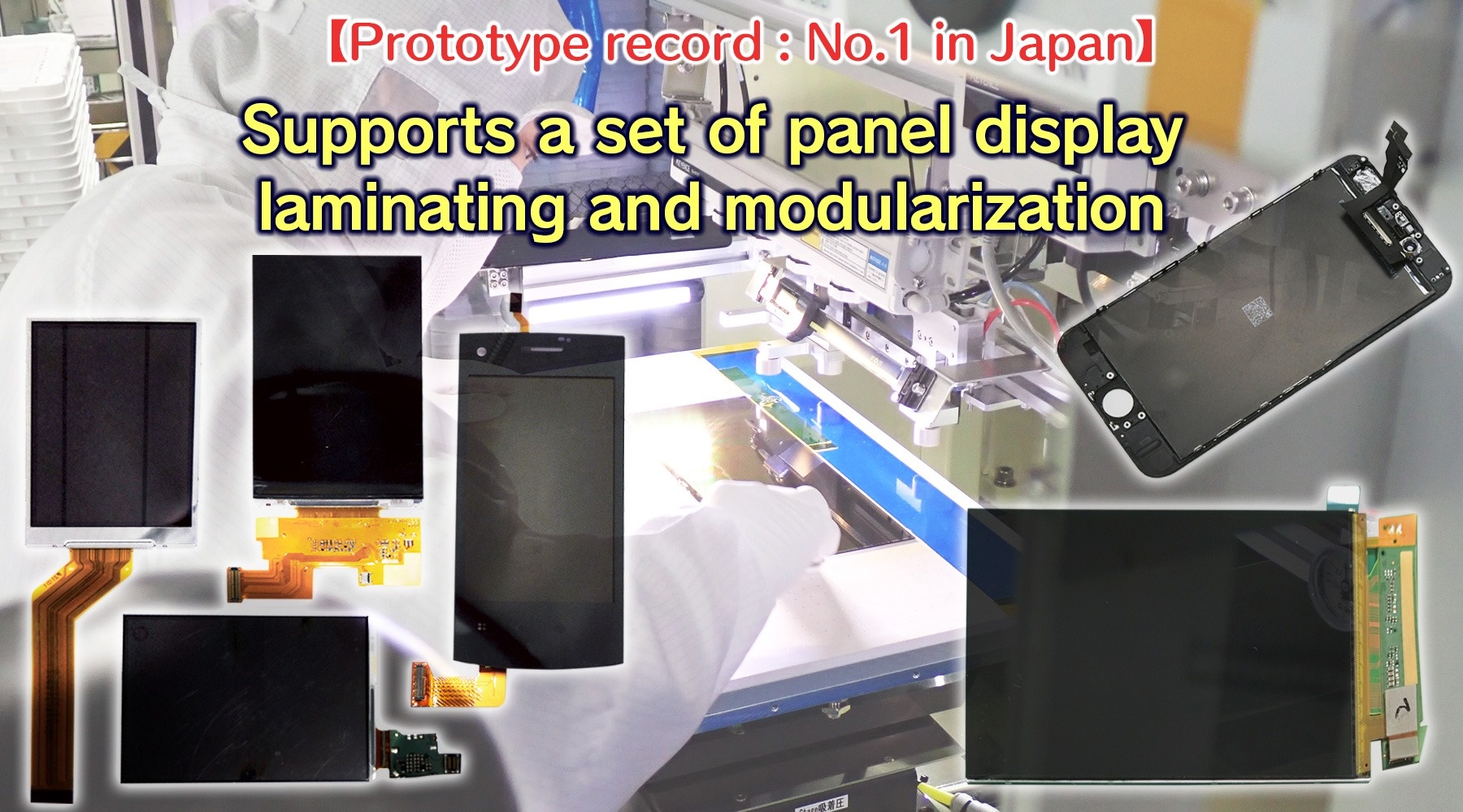
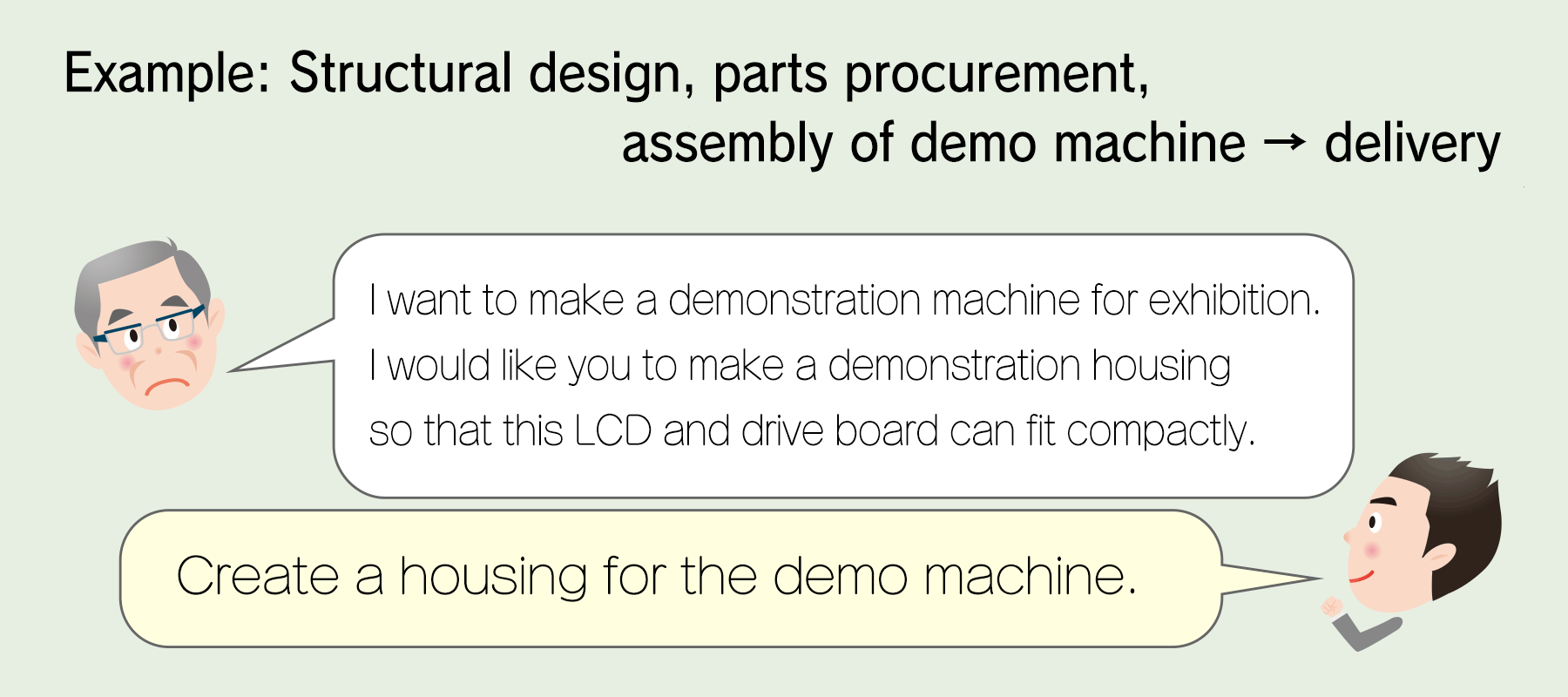
1) Prototype support, trial prototype
The panel and film laminating process supports. Trial production from a single panel.
Please contact us for the difficult prototype requirements that other companies have refused. We will try the prototype after considering the machine and process.
2) Consultation advice on technology and manufacturing process
We will build and realize the optimum laminating process based on many prototype results and experience values for highly difficult laminating such as high precision, various materials, and curved surfaces.
We also provide feedback on prototype results upon request. Please contact us if you have any information that requires feedback on the evaluation of the prototype.
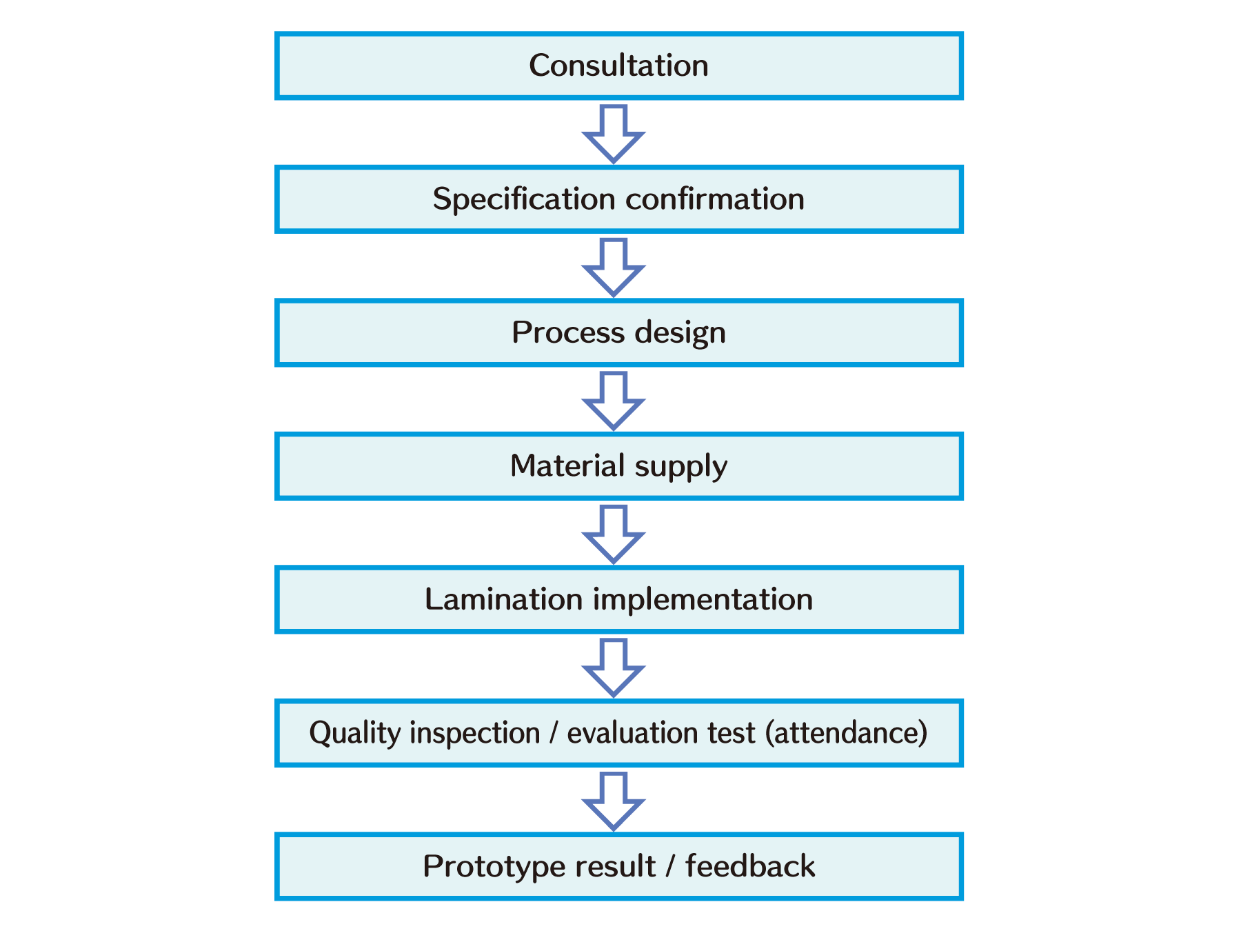
Prototype implementation flow
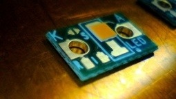
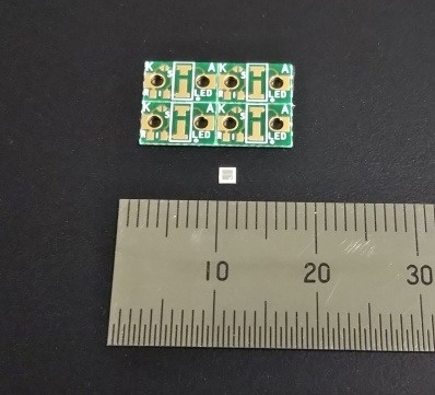
Laminating example
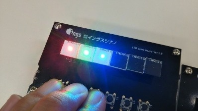
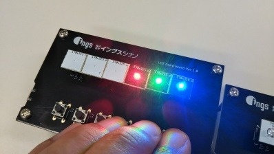
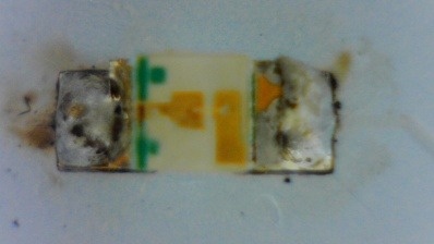
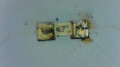
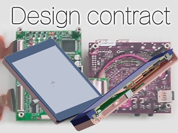
LCD module with touch panel (prototype / mass production)
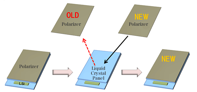
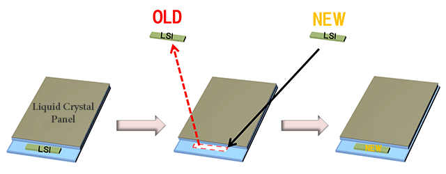
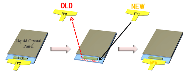
- Laminating a polarizing plate to the liquid crystal panel(Right figure: 1 and 2)
- Laminating of cover glass and touch panel(Right figure: 3 and 4) Both film and glass can be laminated together.
- Laminating of LCD module and touch panel module(Right figure: 2 and 3)
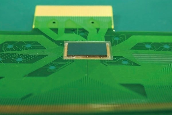
Laminating heater film (prototype / mass production)
A film heater is laminated to the cover material.
It is attached to a flat surface or curved surface with the take-out wire such as harness and FPC attached.
Laminating heat ray reflective film for HUD (prototype / mass production)
A heat ray reflective film is laminated to prevent the infrared (IR) component of sunlight from entering the HUD optical system.
Laminate of film OLED to cover material (prototype)
Laminate of film OLED to 2.5D curved cover.
Experienced in both concave and convex shapes.
Laminating AR film to 3D glass (prototype / mass production)
Anti-reflective film (AR Film) is laminated to 100 x 150 mm R2000 class 3D glass.
Film laminate to S-shaped member (prototype)
A piece of film is laminated to the S-shaped member.
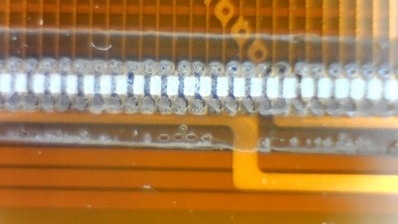
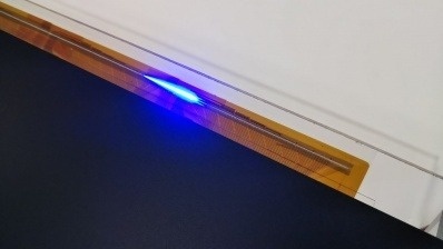
Direct laminating of multiple displays (prototype)
Direct laminating of multiple LCD modules to 1000mm class elongated glass.
In-vehicle cluster display-CID is realized with one material.
Laminating prototype with different optical films (prototype)
We are prototyping different materials for the protective film used to protect materials, which is compatible with polarized sunglasses.
We investigate and procure high-performance films such as COP, TAC, and SRF, and laminate them to the parts.